Hello friends , welcome to ELECTRICAL ENCYCLOPEDIA. In this article we will study about the Parallel Adder.
In most of the logic circuit, addition of more than 1 bit is carried out which can be accomplished by using several full adders. "Number of full adders required is equal to the number of bits to be added". For eg- for adding two 4-bit number we will require 4 full adders which will generate a 4-bit sum and a carry output.
All the bits of the augend (number A) and addend (number B) are fed into the adder circuit simultaneously.
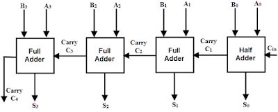
As shown in the figure below is a 4 bit parallel adder.
1. The least significant bit (LSB) i.e, A₀ , B₀ and C₀ (which is initially 0) are added and results in S₀ and C₁. This carry C₁ becomes the carry input to the second stage.
2. Similarly, in the second stage A₁,B₁ and C₁ are added resulting in S₁ and C₂.This carry C₂ becomes the carry input to the third stage.
3. In the third stage A₂,B₂ and C₂ are added resulting in S₂ and C₃. This carry C₃ becomes the carry input to the fourth stage.
4. In the fourth stage, A₃,B₃ and C₃ are added resulting in S₃ and C₄ which is the final output carry. Thus, the circuit results in a sum ( S₃S₂S₁S₀) and a carry output (C₄).
Note that since the parallel adder have simple circuit but its speed of operation is limited because for the operation of each full adder, it requires the carry input from the previous state, this creates a carry propagation delay through all stages (full adder).
Thanks for reading.
Keep Sharing & loving.
In most of the logic circuit, addition of more than 1 bit is carried out which can be accomplished by using several full adders. "Number of full adders required is equal to the number of bits to be added". For eg- for adding two 4-bit number we will require 4 full adders which will generate a 4-bit sum and a carry output.
All the bits of the augend (number A) and addend (number B) are fed into the adder circuit simultaneously.
As shown in the figure below is a 4 bit parallel adder.
 |
| 4 BIT PARALLEL ADDER |
WORKING OF PARALLEL ADDER.
It consists of 4 full adder and input to the each full adder is Ai , Bi and Ci, and the output will be Si and Ci₊₁. The carry output of the lower order stage is connected to the carry input of the next higher order stage.1. The least significant bit (LSB) i.e, A₀ , B₀ and C₀ (which is initially 0) are added and results in S₀ and C₁. This carry C₁ becomes the carry input to the second stage.
2. Similarly, in the second stage A₁,B₁ and C₁ are added resulting in S₁ and C₂.This carry C₂ becomes the carry input to the third stage.
3. In the third stage A₂,B₂ and C₂ are added resulting in S₂ and C₃. This carry C₃ becomes the carry input to the fourth stage.
4. In the fourth stage, A₃,B₃ and C₃ are added resulting in S₃ and C₄ which is the final output carry. Thus, the circuit results in a sum ( S₃S₂S₁S₀) and a carry output (C₄).
Note that since the parallel adder have simple circuit but its speed of operation is limited because for the operation of each full adder, it requires the carry input from the previous state, this creates a carry propagation delay through all stages (full adder).
Thanks for reading.
Keep Sharing & loving.